Stay Connected
Receive product updates and event notifications
Subscribe to Our NewsletterFormFactor is a leading provider of essential test and measurement technologies along the full IC life cycle – from characterization, modeling, reliability, and design de-bug, to qualification and production test.
Receive product updates and event notifications
Subscribe to Our NewsletterEasy – flexible – future proof: Customize your 150 mm manual probe station with application-specific starter kits.
Whatever the application - device characterization, modeling, process development, design de-bug or IC failure analysis, 200 mm manual and automated wafer probe stations have the precision and versatility needed for the most advanced semiconductor processes and aggressively scaled devices.
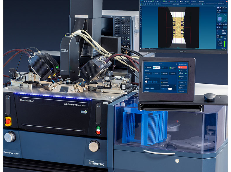
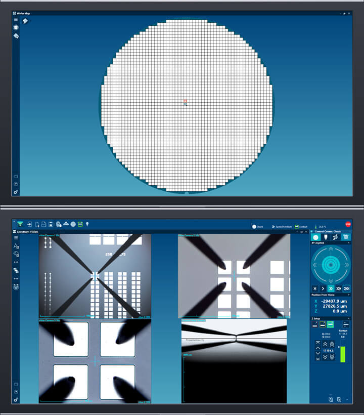
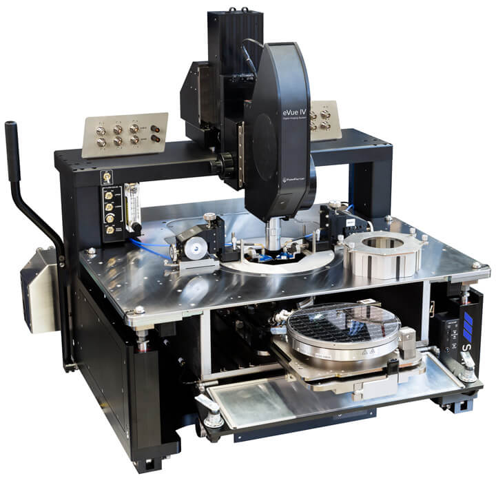
Advanced 200 mm semi-/ fully-automated probe system
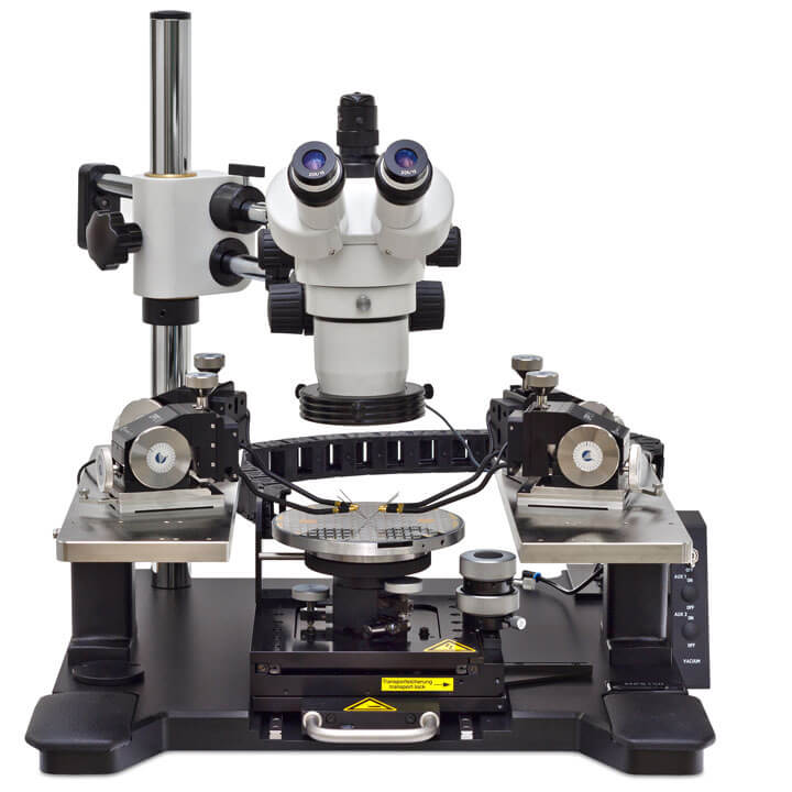
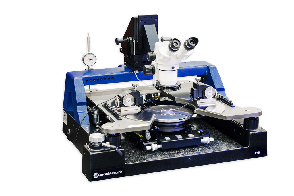
200 mm manual probe system
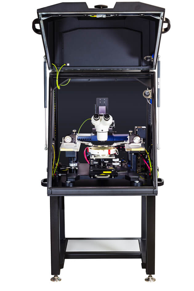
200 mm manual open probe system
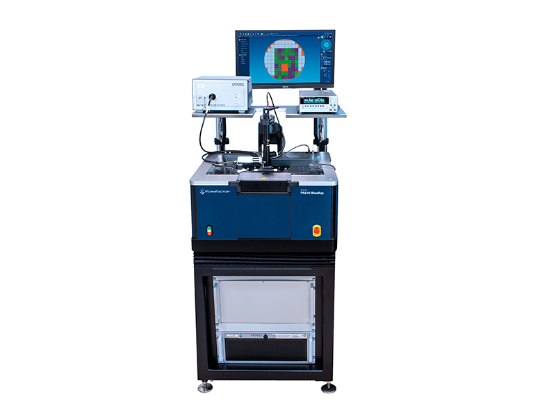
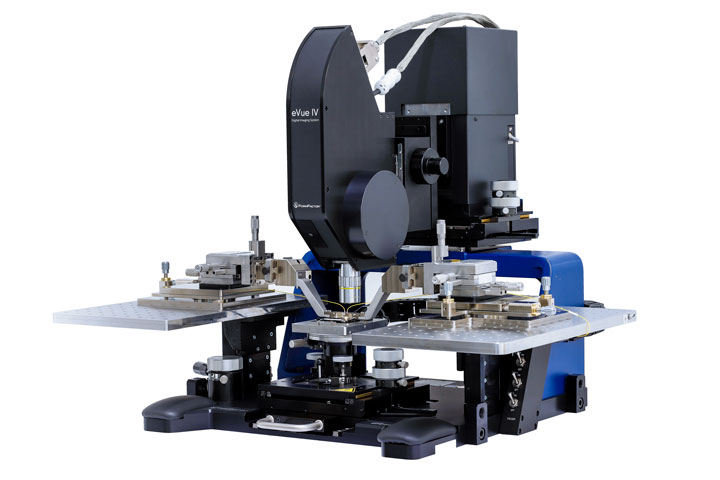
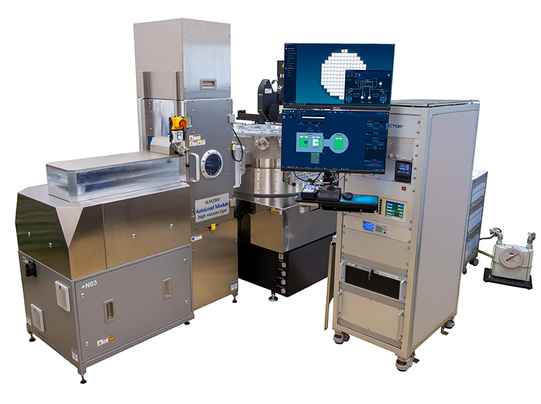
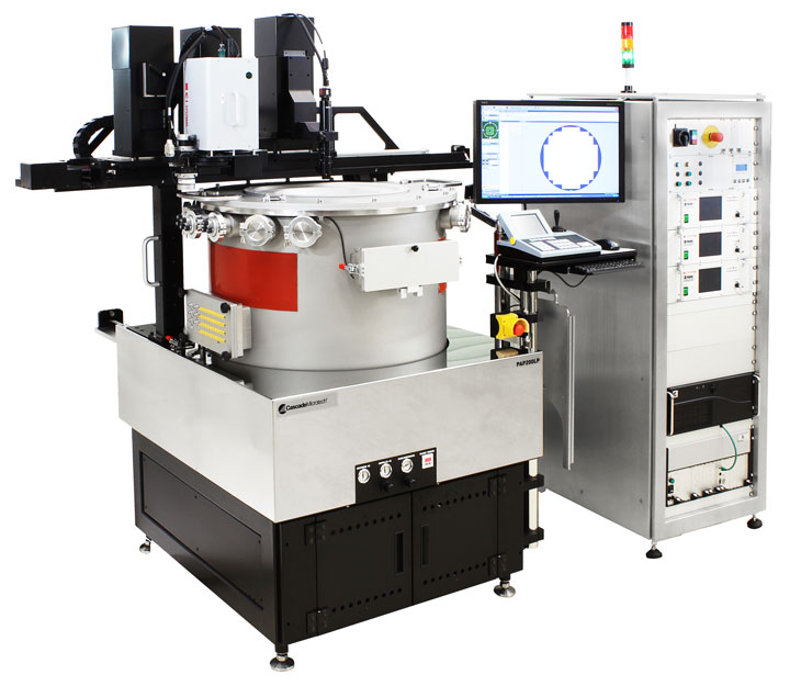
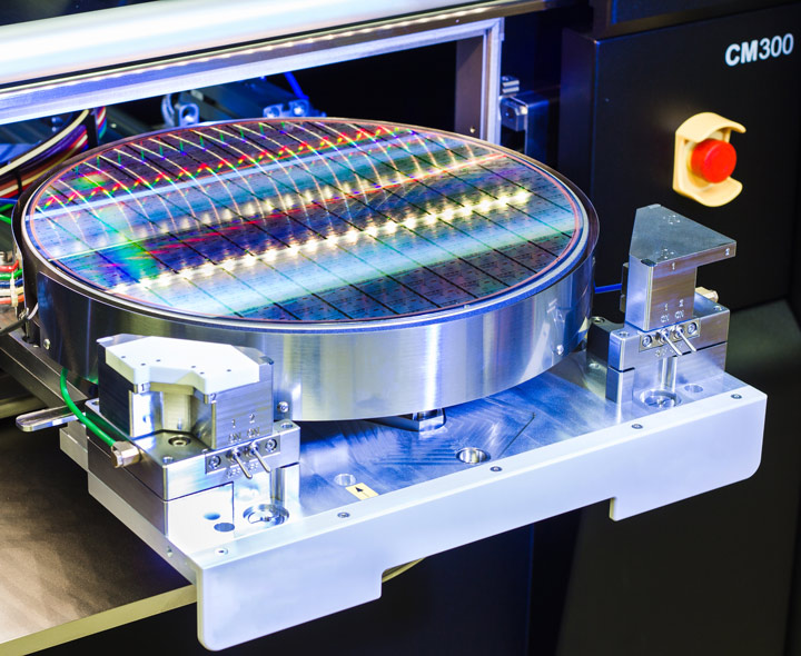
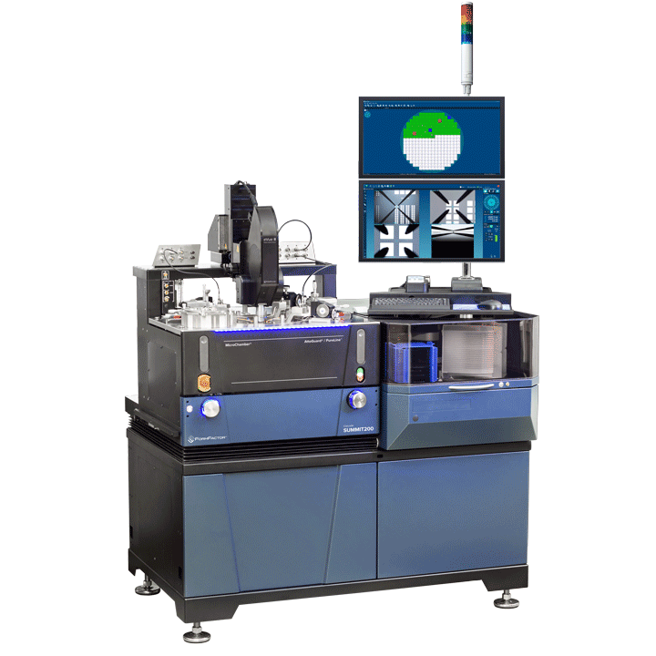
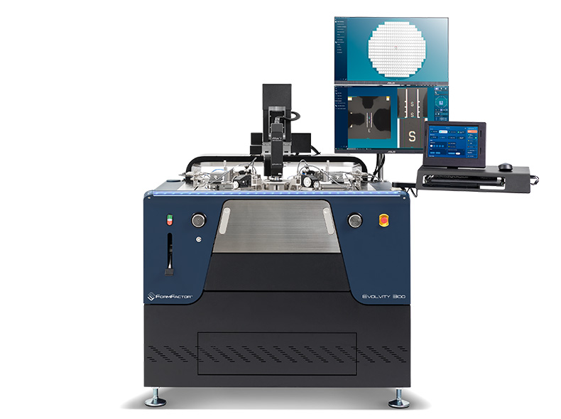
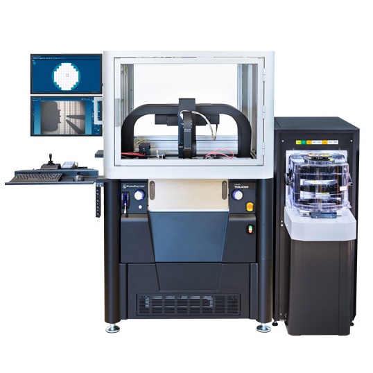
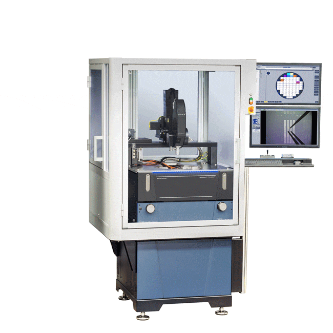
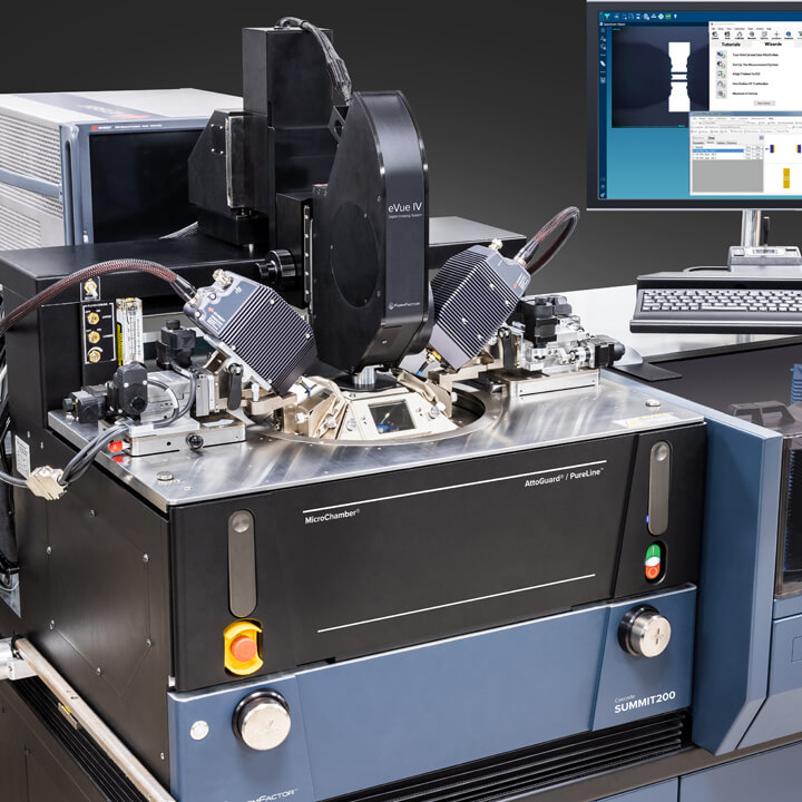
200 mm semi-/ fully-automated production probe system
200 mm manual probe system for RF test up to 67 GHz
mmW probing up to THz and load-pull
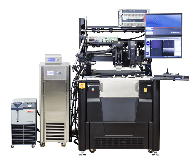
Cascade 300 mm probe stations set the standard for manual and automated on-wafer test, delivering the precision and versatility needed to address a wide range of advanced, complex testing requirements.
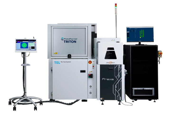
Production-ready silicon photonics test cell
300 mm semi-automated probe system
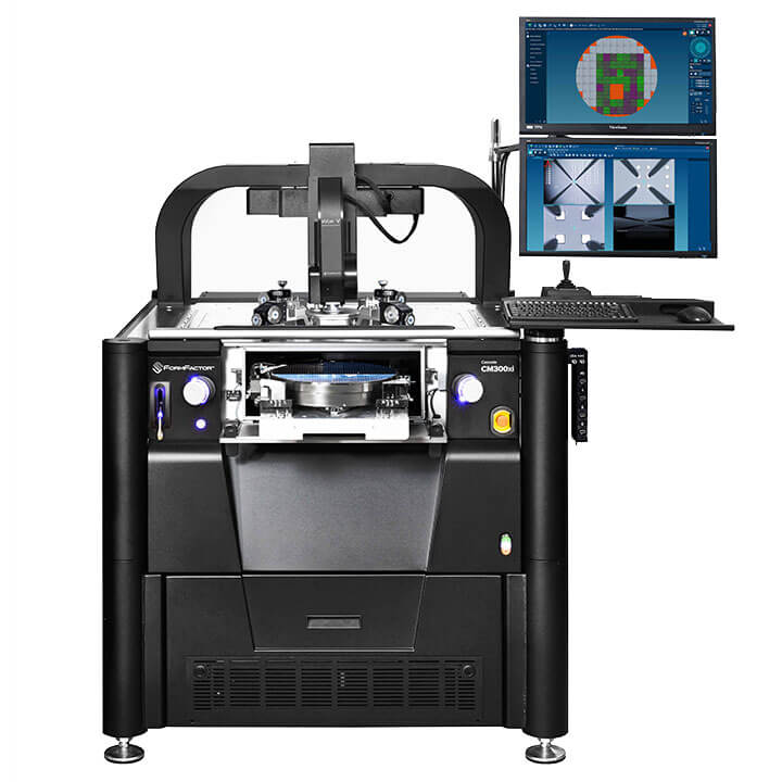
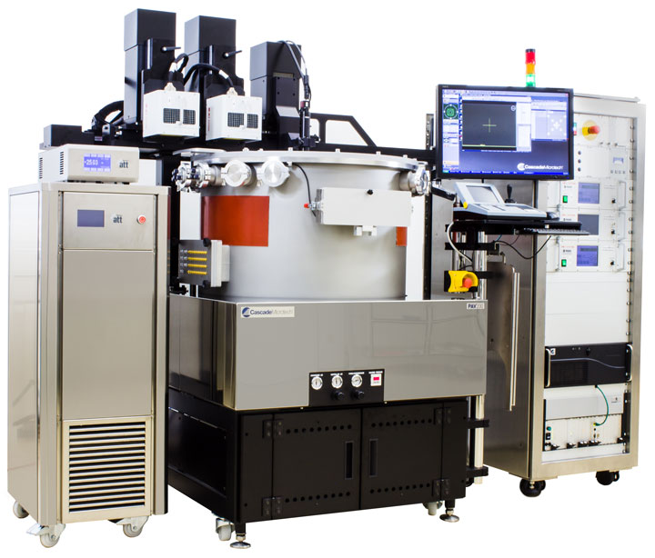
300 mm semi-/ fully-automated probe system
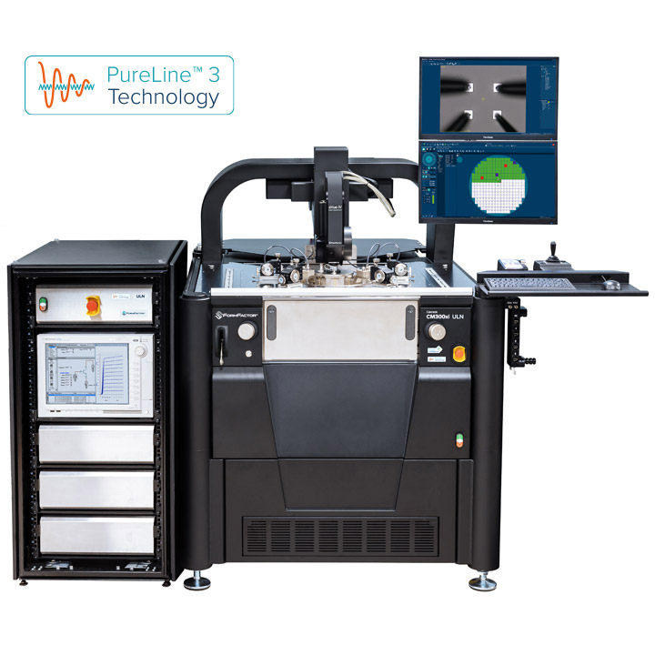
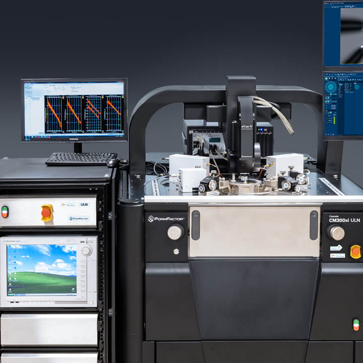
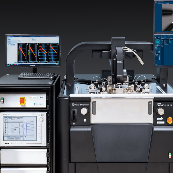
300 mm semi-/ fully-automated probe system for Ultra Low Noise measurements
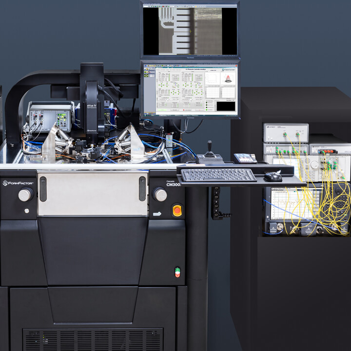
300 mm semi-/ fully-automated probe system with Autonomous Silicon Photonics Measurement Assistant
300 mm semi-/ fully-automated on-wafer power device characterization system
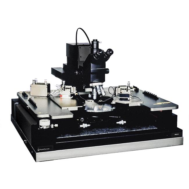
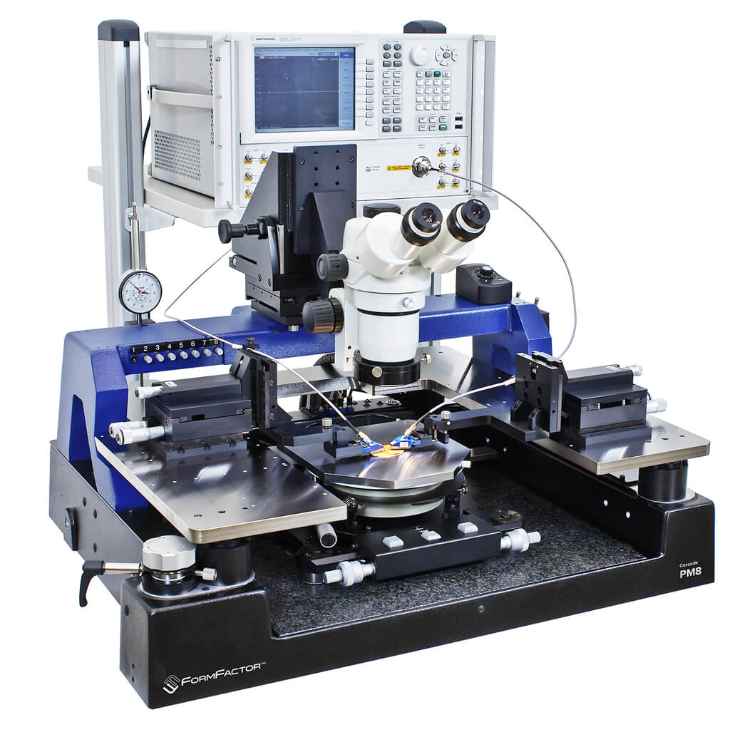
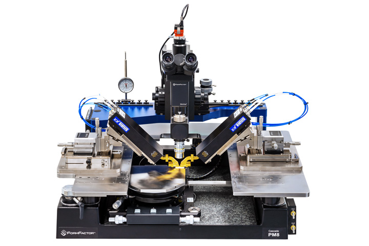
300 mm manual probe system
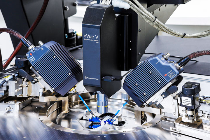
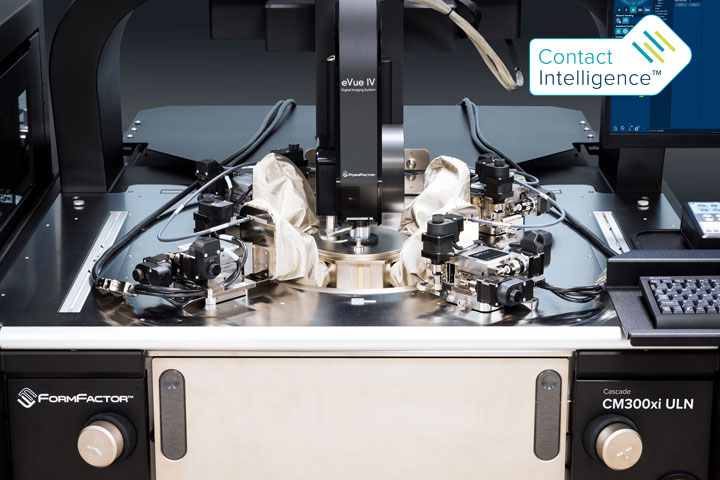
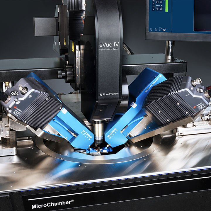
FormFactor’s Contact Intelligence technology combines smart hardware design and innovative software algorithms to provide accurate probe-to-pad alignment and electronic recalibrations in engineering labs and many production applications. FormFactor now has specialized Contact Intelligence assistants for autonomous RF, DC and Silicon Photonics (SiPh) testing.
Autonomous High-Power wafer probing featuring Contact Intelligence
Autonomous DC wafer probing featuring Contact Intelligence
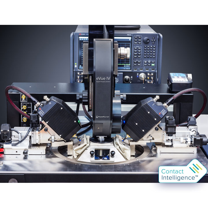
Autonomous RF wafer probing featuring Contact Intelligence
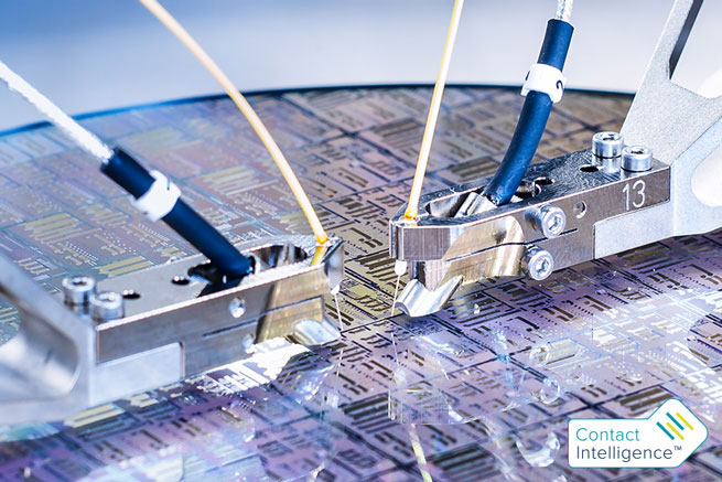
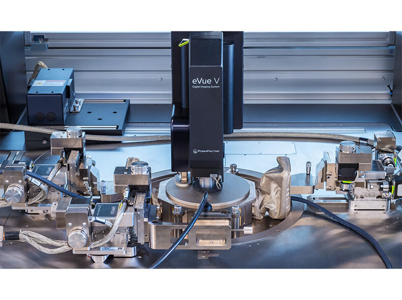
Autonomous SiPh wafer probing featuring Contact Intelligence
The broad use of power semiconductors has created a pressing need to characterize power devices quickly and efficiently. FormFactor offers on-wafer power device characterization systems to reduce time-to-market for new power devices and to keep up with production.
Autonomous High-Power wafer probing featuring Contact Intelligence
300 mm semi-/ fully-automated on-wafer power device characterization system
200 mm semi-/ fully-automated on-wafer power device characterization system
150 mm manual on-wafer power device characterization system
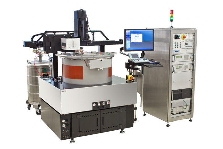
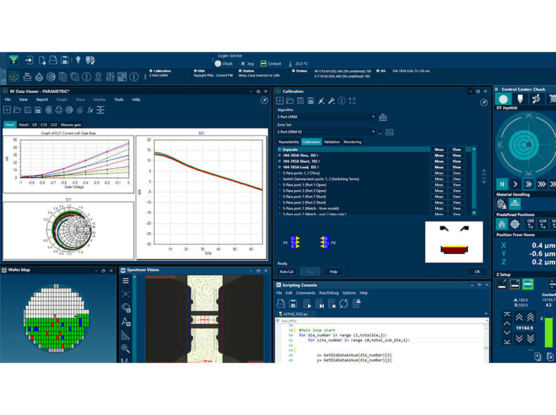
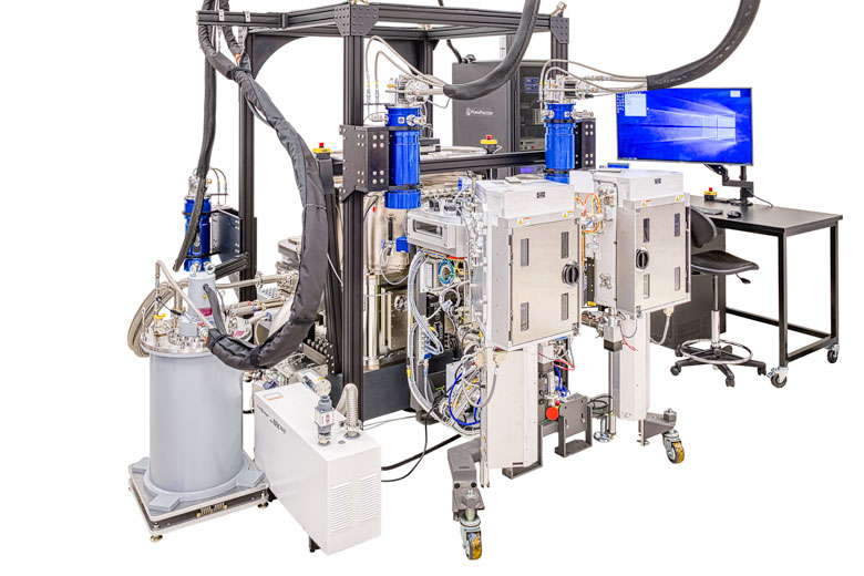
FormFactor’s IMS products deliver robust, turn-key functionality, peace of mind, and a faster path to collecting high-quality on-wafer measurement data for today’s important and challenging test applications. Integrated Measurement Systems unite instruments and other products from FormFactor’s partners, including Keysight Technologies, along with FormFactor’s probe systems, probes, and everything else needed to deliver critical data for devices and integrated circuits on the wafer.
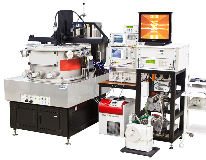
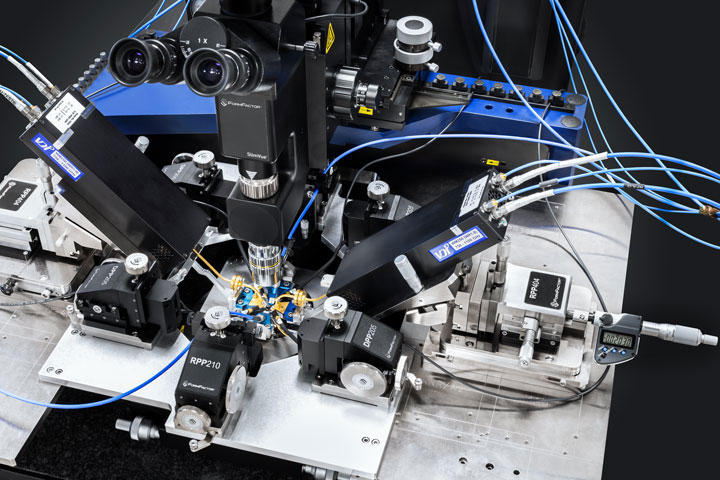
Integrated Measurement System with Keysight VNA for S-parameters from RF to mmW to THz
Integrated Measurement System with Keysight VNAs and Focus Microwaves tuners for On-Wafer Load-Pull Measurements
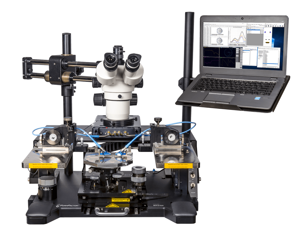
Integrated system with Keysight A-LFNA for 1/f flicker noise, RTN, phase noise, device characterization, and other low-frequency noise measurements
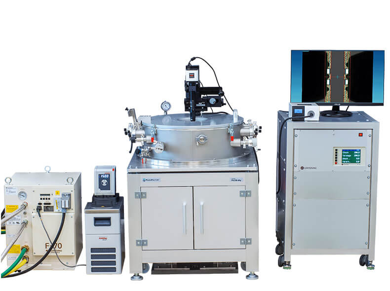
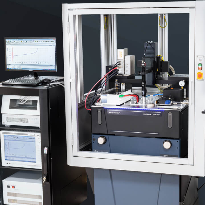
Cryogenic Low Frequency Noise Prober
Integrated system with Keysight SPA for DC parametric measurements
Integrated system with Keysight PDA for power semiconductor device characterization
Integrated system with Keysight Photonics Application Suite hardware and software
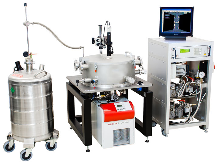
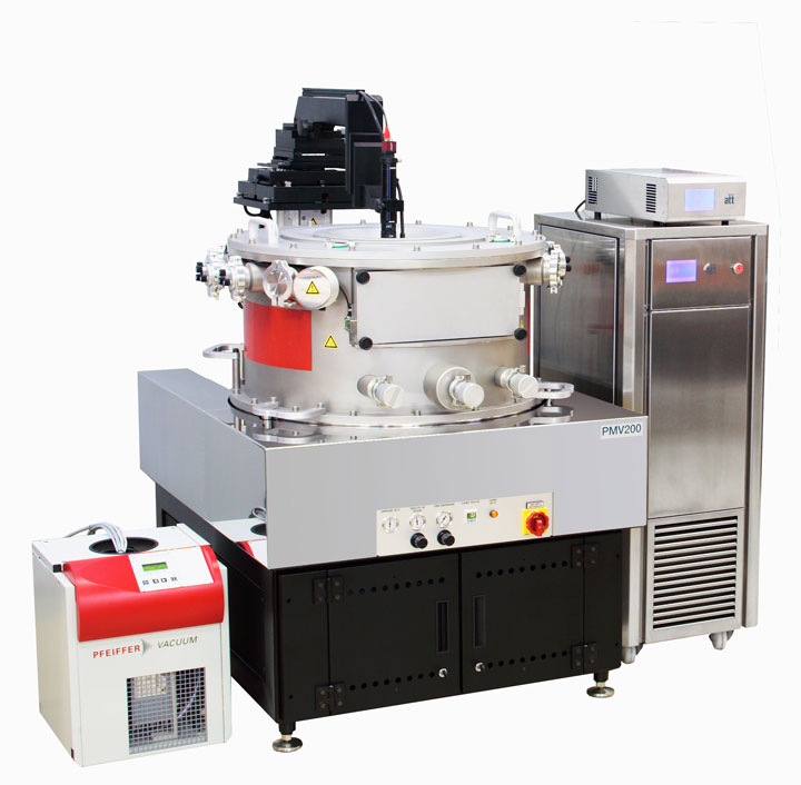
Our high-performance cryogenic probe stations for on-wafer and multi-chip measurements support a wide range of challenging applications, including IR-sensor test, radiometric test, DC and RF measurements at cryogenic temperatures. The systems can handle wafers up to 300 mm, and support cold filter, cold shutter and selectable f/value aperture as well as multiple optical instruments like IR radiation sources (black bodies). Up to eight probe positioners and/or a probe card can be integrated. Automatic chip alignment, OCR and wafer mark reading are exclusive features of our fully- and semi-automated systems. Cooling options include liquid helium (LHe), liquid nitrogen (LN2) or cryogen-free cooling. With a large install base of >80 stations worldwide, we bring expertise and technical know-how to provide the right solution for your measurement challenge.
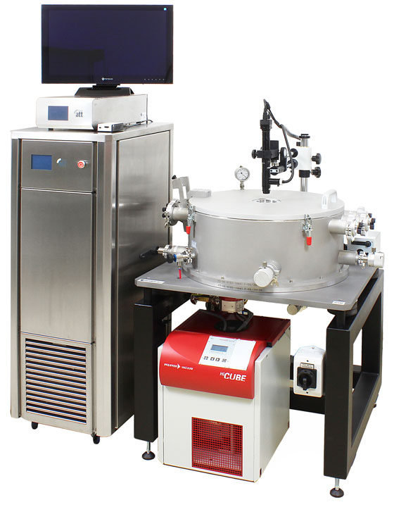
Our vacuum and pressure probe stations for on-wafer measurements in a high vacuum or controlled pressure environment enable precise µ-bolometer test (un-cooled IR-FPA), MEMS characterization (inertial MEMS, resonators and RF MEMS, pressure sensors), IV/CV, RF/mmW and Opto measurements. Multiple optical instruments like IR radiation sources (black bodies), and up to eight probe positioners and/or a probe card can be integrated. The high stability design provides excellent contact quality and accurate measurement results in a condensation-free test environment. Step and repeat capability enables high throughput with our semi-automated systems.
Customized solutions for a variety of challenging applications
We offer several unique software solutions that enhance the functionality of your wafer-level test system
Receive product updates and event notifications
Subscribe to Our Newsletter