Stay Connected
Receive product updates and event notifications
Subscribe to Our NewsletterFormFactor is a leading provider of essential test and measurement technologies along the full IC life cycle – from characterization, modeling, reliability, and design de-bug, to qualification and production test.
Receive product updates and event notifications
Subscribe to Our NewsletterThe latest DRAM chips deliver extremely fast and smooth graphic and cache memory response in game consoles and personal computers, as well as server applications. They afford soaring memory capacity in smaller and smaller cellular phones, IOT and other consumer electronics, as semiconductors get stacked into compact packages of multi-tasking die. Testing these new, high-performance, high-density DRAM devices is optimized with FormFactor’s Matrix and PH-Series wafer probe cards as they improve efficiency and reduce the overall cost of DRAM test.
Fluctuating price and demand routinely require Flash memory manufacturers to find new operating efficiencies. FormFactor advanced wafer test solutions help manufacturers address that pressure, by improving yield and reducing overall cost of test per die.
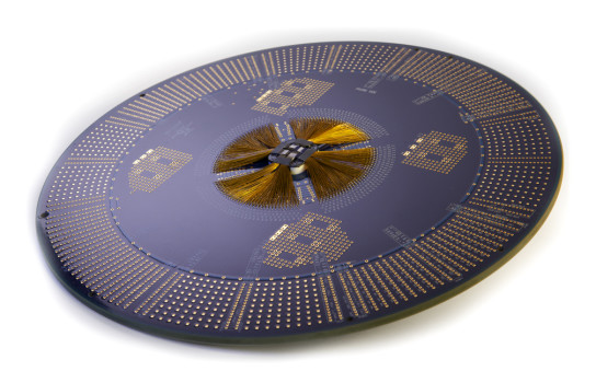
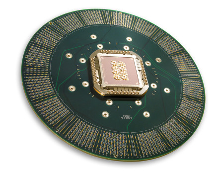
Wearables, smart phones and Internet of Things (IOT) are driving devices that are small, have high performance and long battery life. The logic chips used to drive these applications use advanced packaging technologies such as flip-chip, and wafer-level packaging in smaller form factor and higher electrical performance. Growing use of semiconductors in automobiles drive an increased need for reliability, safety and higher operating ranges than consumer devices. Apollo, Altius, Katana probe cards from Formfactor enable testing of logic devices at finer pitches, higher temperatures and increased parallelism to lower the cost of test and increased assurance to customer of delivery of a reliable product.
Enables test of high performance very large I/O logic devices with fine pitch micro-bumps
High parallelism, vertical probe card for automotive and industrial devices
For advanced wafer-level chip scale packaged (WLCSP) devices with a pitch range of 250-500μm
Wafer test probe cards for fine pitch, wire bond logic devices
Designed for fine-pitch flip-chip applications with high current carrying capability - copper pillar and solder bumps
For advanced wire bond logic and SoC devices
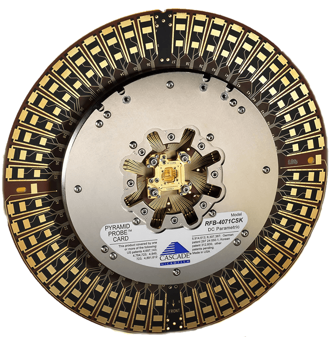
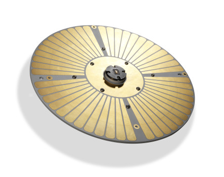
Pyramid RF Probe cards provide best-in class RF performance and maintain exceptional signal integrity from the tester interface to the die for semiconductor wafer test. Capable of probing beyond 80 GHz, Pyramid probes provide the highest fidelity measurements for RF applications. Pyramid is capable of both high-volume manufacturing and engineering applications due to its minimal pad damage and low probe inductance. FormFactor’s Pyramid probes have the lowest ground inductance available in a probe card allowing for optimized RF measurements of any RF application from cell phone RF Front End parts to Automotive Radar chips.
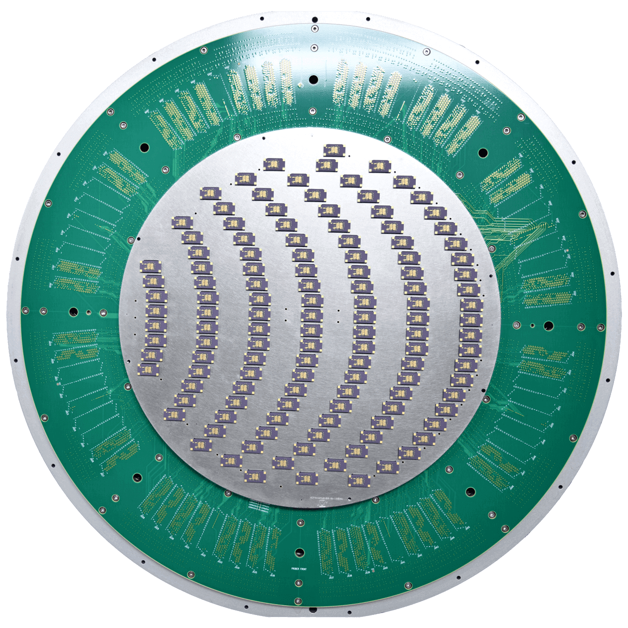
FormFactor’s family of optical device probe cards offer customized solutions for testing CMOS image sensors and LED devices. FormFactor’s Hikari probe card solution delivers excellent light uniformity, low power noise within the DUT and across the array, with minimal pad damage. Akari probe cards, with both multi-site and single-site/2-pin options, deliver a high-precision test solution for LEDs. These capabilities allow manufacturers to reduce test time and maximize yields.
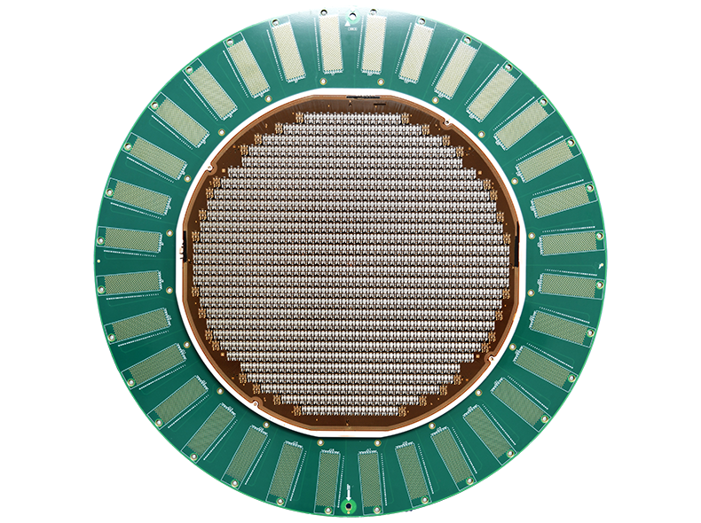
Takumi™ probe cards for in-line and end-of-line parametric testing give IC manufacturers earlier insight into opportunities to validate their designs, verify process performance and achieve higher yields. High contact precision supports manufacturers’ use of smaller test pads and narrower scribe lines on their product wafers.
Millimeter wave frequency transmission and active antenna arrays are the backbone of the emerging 5G capabilities. Formfactor’s Pyramid Probe Card with membrane technology is the only production proven solution in the mmWave range. Pyramid, now with higher parallelism capability is the probing solution for the high RF line counts and low inductance requirements needed for 5G applications.
Production RF probe cards are rugged, robust, and well suited for the rigors of high-performance wafer sort. Their industry-leading signal integrity and mechanical capabilities make these probe cards the perfect fit for multi-die testing for RF wireless and high-speed digital in SiPs and SoCs.
The rapid paced RF Front End market demands high fidelity RF measurement with new design turn times that are much faster than many logic applications. Filters, Switches, PA’s and other sensitive RF devices make up the Front End module in todays smart devices require test solutions that can keep up with the high frequency requirements and offer ongoing improvements in COO. Formfactor Pyramid Probe cards provide industry proven solutions for meeting these requirements today and in the 5G world to come.
In digital communication, timing is the most essential element. Whether this is reflected in a wide open eye diagram, a pico-second rise time, devices working at these speeds need RF performance. Pyramid Probe cards from Formfactor provide demonstrated solutions for all high speed applications including TIA/Driver’s, optical transceivers PAM4 and others with a low inductance, highly isolated test solution.
The combination of stringent automotive market test requirements and millimeter wave performance up to 81GHz demand measurements of the highest quality. FormFactor’s Pyramid technology offers a proven solution in this application with hundreds of cards shipped and a team of RF expertise to ensure the most accurate results.
Receive product updates and event notifications
Subscribe to Our Newsletter